
Kashif Javaid
In this lesson we will focus on a single element Lossless Transmission line (T-line) as shown in Figure 1. Lossless T line simulation will be introduced here. One of the goal of these lessons are to give out practical examples from real world. Transmission line model real world signals very well. This lesson focus on the Lossless T-line where no power gets dissipated during transmission. In a future lesson, we will focus on lossy line and loss mechanics.

Figure 1: LTspice symbol
What is transmission line? A transmission line is any conductor along with a return path where a signal travel from source to load. Because of finite speed of light, a signal takes a finite amount of time called Time Delay (TD) to go from source to load. Signal sees a characteristic impedance (Zo) based on geometry and dielectric around the conductor and return path. For an in-depth review of transmission line, please refer some excellent references as given at the end.
In any simulation we need to build confidence on the models given. One way to do this is find solution of easy problems by hand for cases a formula or numerical values can be derived and then compare them with results from simulation. Once 100% agreement is established, one can go beyond simple situation and start modeling real world effects. In the case of transmission line, let’s look at 4 simple but common cases, where a 50Ω T-line is driven by a CMOS driver with 5Ω source impedance (typical for newer drivers) with an open load, short load, 100Ω load and a properly terminated 50Ω load.
For each case, we will look at the load voltage waveform using bounce diagram. If you haven’t learned or played with bounce diagrams, do not fret, we will walk through it step by step.
First case: Load = Open or Hi-Z
For an open load situation, let’s start to build a bounce or reflection diagram for the below open circuit:

Figure 2: CMOS driver with low impedance driving 50Ω line with no load.
Observations:
- In any circuit, there is signal path and return path which is as important as signal path.
- After the long time meaning several transit time (TD) has been passed, T-line has becomes ideal and since load is open or Hi-Z, voltage at RL will approach 3.3V, after all it’s an open and no current can flow.
- Getting to final 3.3V would take several TD (illustrated below by creating bounce diagram step by step section and LTspice simulation).
- Reflection coefficients at load and source are calculated in Figure 3.
- Reflection coefficient is 1 for an open load case. A
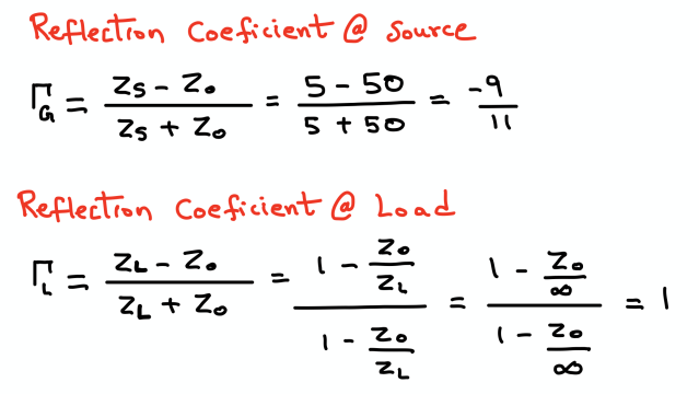 Figure 3: Formula and calculation of Reflection at source and load.
Building Bounce Diagram one TD a time:
Bounce or reflection diagram consist of two axises. Horizontal axis represent location on transmission line and goes from z=0 to z=d where d is actual length of transmission line. Vertical lines represent time and marked as in unit of time delay (TD). We draw a first line representing the signal launched into transmission line. Note V+ and I+ represent the initial waveform voltage and current signal. These signals encounter the impedance of the line, in this case 50Ω. V+ is calculated using the voltage divider formula as 3.3V(50Ω/(50Ω+5Ω)) = 3V and I as V+/Zo.
Similarly V– and I– show reflected voltage and current waveforms respectively. These are calculated using Load reflection coefficient. Similarly V++ and I++ are calculated using generator reflection coefficient and represent reflected waveforms from source after 2 TD. The “tennis match” continues as illustrated in the series of diagrams below:


Figure 4: Building up the bounce diagram
I intentionally picked this example as source and load side impedances are severely mismatched. In-fact load is open with infinite resistance. I think we have enough data to make comparison with LTspice. Here is the load voltage waveform by hand if you were to put an oscilloscope at the load side, this is what we will measured. Of-course, this is not complete as final value should be 3.3V, but it will take several more bounces before it reaches this value, but we let LTspice handle it.
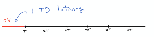


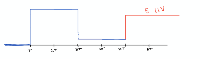
Figure 5: Building up the load voltage waveform
Here are LTspice results:
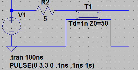

Figure 6: LTspice simulation for open load transmission line
As marked on the waveform, first 6 Time Delay (TD) values are agreed 100% to our calculated values. But notice that it takes several bounces back and forth actually more than 50ns before a steady state value of 3.3V reached. First time I learned this it was really surprising, but it is a direct consequence of finite speed of light and mismatch between source and load impedance.
Second case: Load=0Ω or short
Second interesting case is when load is shorted after the transmission. Since load is shorted, output voltage should be zero, but it will be current that will build up to its final value according to ohm law, I = 3.3V/5 = 0.66A.
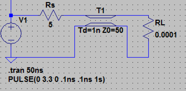
Figure 7: Transmission line for shorted output, note very small value of resistance is used for probing otherwise LTspice won’t give us the current waveform at the load.
Let’s calculate first few TD using the bounce diagram and then we let LTspice calculate the rest of it.


Figure 8: Bounce diagram and current waveform. y-axis is current in Amp and x-axis is time in unit of TD.
Here are LTspice results. Note the agreement between calculated and simulation values. One thing to note is that since we used a very small resistance (just think of resistance of the wire) at the output, voltage will be also climb up like this which you can easily verify it using the attached simulation files.
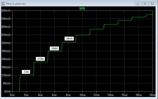
Figure 9: Simulation results of shorted load
Third case: Load=100Ω
This is a typical case where where T-line is driving 50 ohm line with load impedance of 100Ω. 
Figure 9: 50Ω Transmission line driving a 100Ω load
Here is the bounce diagram and LTspice simulation results for this case:
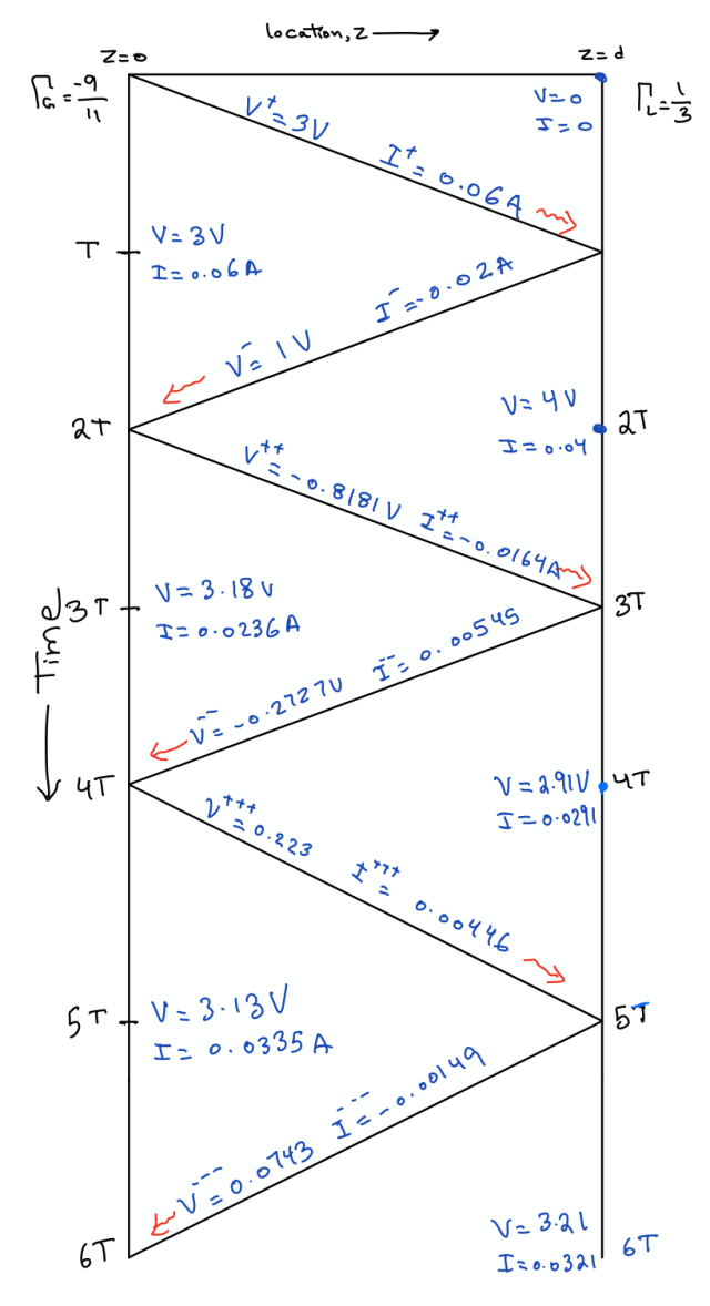

Figure 10: 50Ω Transmission line driving a 100Ω load and its bounce diagram and LTspice simulation results
Fourth case: Load=50Ω
If load is matched with characteristic impedance there will be no reflection and perfect matching will occur. In-fact this is one of a termination scheme in the high speed digital logic circuits. Bounce diagram is very boring, but it show after 1 time delay of latency signal will reach its equivalent value of 3.3*(50/55)=3V. Notice this 50Ω termination has reduce the output voltage by 300mV and will eat up the noise margin. Also, high power consumption is the second factor with this scheme. That’s why other termination schemes are typically employed but this topic warrant its own post.
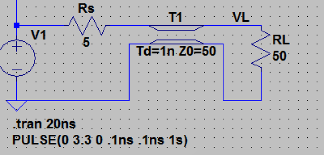
Figure 10: 50Ω Transmission line driving a 50Ω matching load
Here is the bounce diagram:
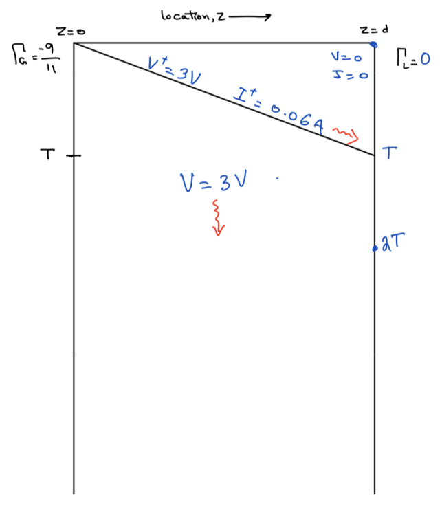
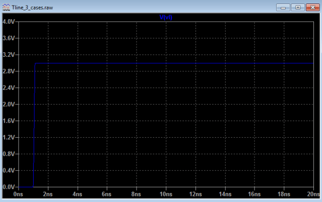
Figure 10: 50Ω Transmission line driving a 50Ω matching load, output voltage, after 1ns of TD, reaches is final value of 3V.
In essence, learning any simulation tool is basically checking fundamental equations and methods against it. Only then one can advance to more complicated and real-world modeling. Hope this post not only show how to simulate transmission line but gives out a good refresher on bounce diagram. Please feel free to post any comments, I will continue to improve on these lessons. Next lesson: Generate Electronic Sources.
Download LTspice file: Tline_3_cases.asc
References:
Gregory D. Durgin, Andrew F. Peterson, Transient Signals on Transmission Lines: An Introduction to Non-Ideal Effects and Signal Integrity Issues in Electrical Systems, ISBN-10: 1598298259
Bogatin, Eric Signal and Power Integrity – Simplified (3rd Edition), ISBN-10: 013451341X
If you want to discuss it then jump here:
https://www.eevblog.com/forum/projects/ltspice-lesson-3-transmission-lines-part-1/new/#new

shouldn’t source impedance be 50 ohm also? you have 5 ohms, why?
5 ohm represent the typical output impedance of a CMOS driver. If you want to eliminate reflection one termination scheme is to match source impedance to line 50ohm, by adding a suitable resistor to make the source impedance look like 50 ohm.
There are mistakes in:
1. Observations point 2, should be RL not VL
2. Figure 3, first part should be RL not RS.
Thank you for pointing out these typos. I have fixed them in the post.
Hi,
Today I’ve found an error in LTSpice with TL simulations. For example, I simulated guanella balun 4:1 from 10cm (330ps length, 25Ohm) TL. 50Ohm in, 12.5Ohm out impedance. Surprisingly I found that it works with almost DC (1Hz..) frequencies. Of course, it’s nonsense, these lines are not coupled at all on that frequency… The S11, S22 for that balun also was perfect on that “DC” frequencies.
If you flip the resistor by 180 degrees in figure 7, you get completely wrong result of zero volts on node between top of resistor and transmission line. It seems resistors behave like they are polarized when connected to transmission line. One way to get around is to ground both sides of the transmission line instead of just one side. It’s not correct in real-world sense, but it does give correct result in ideal T-line as used in simulation.
HSpice shows how they model lossless T-Line using voltage source, and they would have a problem with Fig 7 type of connection.
Click to access chapter_21.pdf
But that doesn’t explain why LTSpice resistor behave completely wrong when flipped. I can’t find any documentation on how LTSpice models lossless T-Line.
Hi There!
Can someone please guide me through my design project. Thank you!
Lab#2: Narrowband microwave amplifier design
Objective:
•To design, construct, simulate, and test a small-signal, high-frequency amplifier.
Design a narrow band amplifier at 5 GHz using the UFET model of Figure 1.
The design should follow the general input/output matching circuit approach of Figure 2 with the various topology options. You are free to choose any circuit topology you wish. However, I would prefer a stub-based design. I also suggest you choose solutions that require the minimum line lengths for both the
series and shunt lines. You may make use of the Smith chart to design the matching circuit.
Figure 2: Narrow band amplifier design using input and output impedance matching circuits. Γ𝑠=Γ𝑖∗ and Γ𝐿=Γ𝑜∗.
To obtain values for Γ𝐼 and Γ𝑂 use the provided LTspice schematic UFET model shown in Figure 3.
Figure 3: Test circuit for measuring for Γ𝐼 and Γ𝑂.
In the results, show the relevant measurements (multimeter and oscilloscope plots) as proof that the circuit is operating as intended.
That was a really interesting and enlightening read, thank you Kashif.